

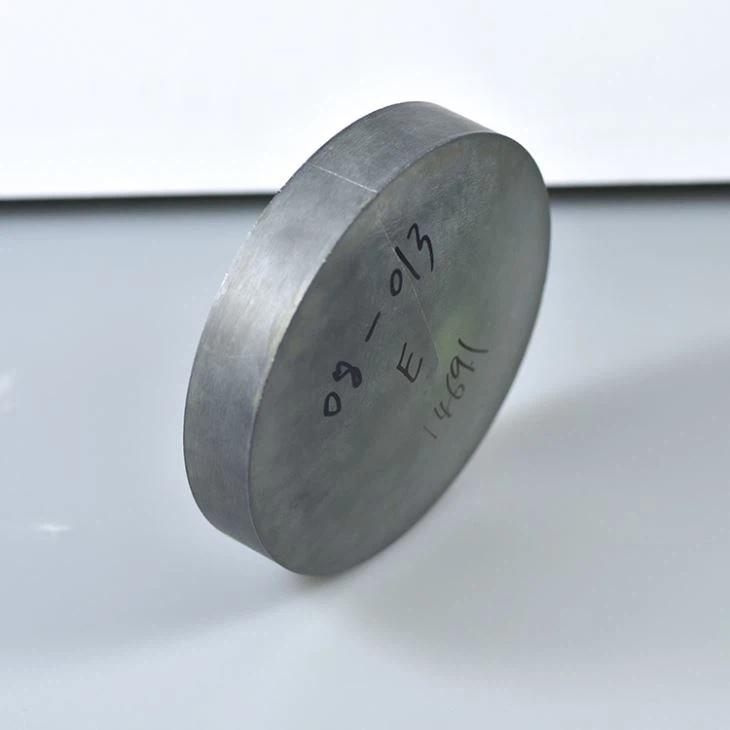
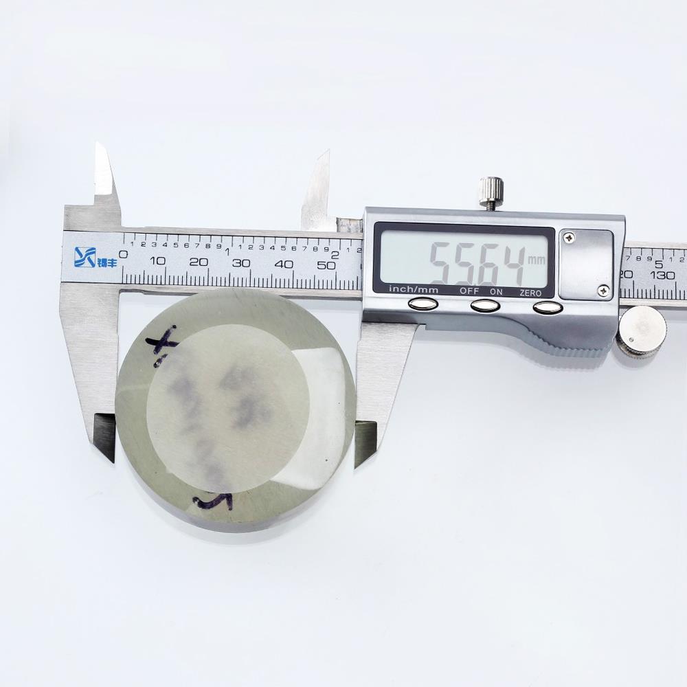
Silicon Carbide Wafer
Description
Technical Parameters
A wafer, also called a slice or substrate, is a thin slice of semiconductor material, such as a crystalline silicon, used in electronics for the fabrication of integrated circuits and in photovoltaics for conventional, wafer-based solar cells. The wafer serves as the substrate for microelectronic devices built in and over the wafer and undergoes many microfabrication process steps such as doping or ion implantation, etching, deposition of various materials, and photolithographic patterning. Finally, the individual microcircuits are separated (dicing) and packaged.
By 1960, silicon wafers were being manufactured in the U.S. by companies such as MEMC/SunEdison. In 1965, American engineers Eric O. Ernst, Donald J. Hurd, and Gerard Seeley, while working under IBM, filed Patent US3423629A for the first high-capacity epitaxial apparatus.
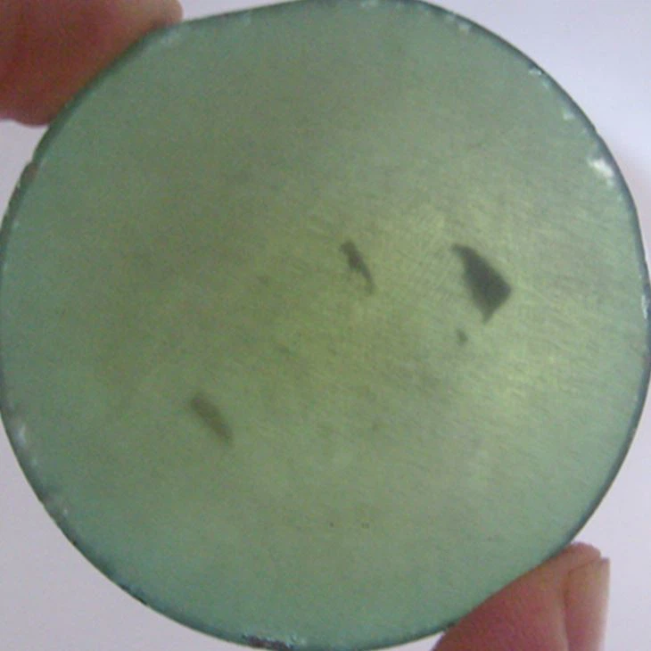
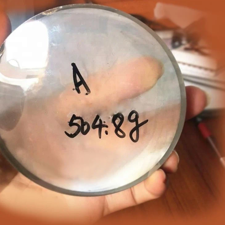
Hmois moissanite crystal can be done to all kinds of moissanite jewelry, like moissanite ring, moissanite pendant, moissanite bracelet and other moissanite products.
Physical Properties of Moissanite
Lustre: Vitreous
Transparency: Transparent
Colour: Green, black, blue, colourless, green yellow, yellow
Streak: Greenish grey
Hardness: 9½ on Mohs scale
Cleavage: Poor/Indistinct
{0001} Indistinct
Fracture: Conchoidal
Density: 3.218 - 3.22 g/cm3 (Measured)
Comment: 3.218 - 3.22, Average = 3.21
Chemical Properties of Moissanite
Formula: SiC
Elements listed: C, Si - search for minerals with similar chemistry
|
Properities |
Moissanite |
|
Chemical Component |
High purity SiC |
|
Refraction |
2.7 |
|
Relative Density |
3.2 |
|
Dispersion |
0.104 |
|
Hardness |
450GPa(NOTE: Diamond should be 1050GPa) |
|
Thermal Conductivity |
390W/M/K |
|
Thermal Coefficient of Expansion |
3*10-6/K |
|
Transmittance |
400 Nano to Far TR |
|
Electrical Resistivity |
Between 103-1012 |
|
Product |
4H-SiC & 6H-SiC |
||
|
Grade |
Grade l |
Grade ll |
|
|
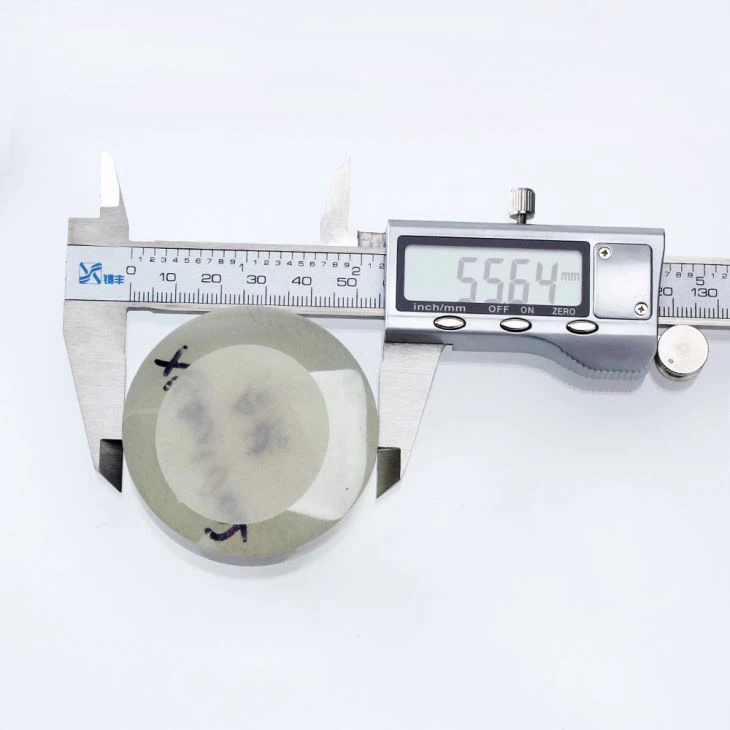
Diameter |
50.8mm±0.38mm |
||
|
Thickness |
8mm- or Customer Specification |
||
|
Primary Flat Orientation |
Perpendicular to <11-20>±5.0︒ |
||
|
Primary Flat Length |
15.88mm±1.65mm |
||
|
Secondary Flat Orientation |
90°CW from Primary flat±5.0° |
||
|
Secondary Flat Length |
8.0m±1.65mm |
||
|
Positive Angle chip direction |
{0001}±0.28 |
||
|
Off axis Wafer Orientation |
4.0°toward<11-20>±0.5° |
||
|
Edge Exclusion |
1.0㎜ |
||
|
TTV/Bow |
<15um/<15um |
||
|
Micropipe Density |
<10piece cm-2 |
<30piece/cm-2 |
|
|
Resistivity |
Conductive |
0.01-0.03 |
0.01-0.1 |
| Semi-insulating |
>105 ×cm ×cm
|
||
|
Surface Finish |
Both Polished (Si face Ra <0.2nm) or Customer Specification |
||


Use of our moissanite crystal, rough moissanite

Standard wafer sizes
Silicon wafers are available in a variety of diameters from 25.4 mm (1 inch) to 300 mm (11.8 inches). Semiconductor fabrication plants, colloquially known as fabs, are defined by the diameter of wafers that they are tooled to produce. The diameter has gradually increased to improve throughput and reduce cost with the current state-of-the-art fab using 300 mm, with a proposal to adopt 450 mm. Intel, TSMC and Samsung are separately conducting research to the advent of 450 mm "prototype" (research) fabs, though serious hurdles remain.
2-inch (51 mm), 4-inch (100 mm), 6-inch (150 mm), and 8-inch (200 mm) wafers
1-inch (25 mm)
2-inch (51 mm) with thickness 275 µm.
3-inch (76 mm) with thickness 375 µm.
4-inch (100 mm) with thickness 525 µm. Or 4.9 inch (125 mm) with thickness 625 µm.
150 mm (5.9 inch, usually referred to as "6 inch") with thickness 675 µm.
200 mm (7.9 inch, usually referred to as "8 inch") with thickness 725 µm.
300 mm (11.8 inch, usually referred to as "12 inch") with thickness 775 µm.
450 mm (17.7 inch) with thickness 925 µm (proposed).[15]
675-millimetre (26.6 in) Unknown thickness. (Theroretical).[16]
Wafers grown using materials other than silicon will have different thicknesses than a silicon wafer of the same diameter. Wafer thickness is determined by the mechanical strength of the material used; the wafer must be thick enough to support its own weight without cracking during handling.
Machine of our moissanite crystal, rough moissanite

Factory of our moissanite crystal, rough moissanite

Exhibition of our company
Bangkok Gem&Jewelry Fair 62nd

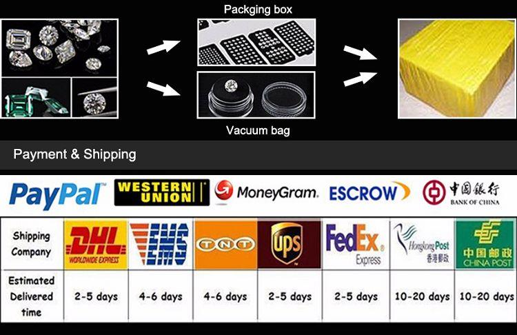
Package and shipment and payment

Why choose us:
(1. 30 sets of advanced imorted and national cutting machine
(2. fashion, latest design, always catch the latest fashion
(3. Unique styles, excellent quality and considerate services win general customers’ unanimous recognition and praise. We adhere to the management idea of regarding quality as life, innovation as driving force and customer first!
(4. Your visit to our company will be great honor! We are looking forward to your cooperation! Let’s work together for mutual development!
Moissanite Maintenance
The Moissanite ring should be removed when doing heavy work, so as to avoid the deformation of the ring and the Mosang stone.Maintenance Moissanite ring, professional cleaning: Moissanite stone is very lipophilic and easy to contaminate oil, so apply hand cream and remove Moissanite when washing dishes. It can't be worn while swimming, and the chloride bleach in the water will erode the Moissanitering. It is recommended to choose professional jewelry cleaners and instrument cleaning. Maintenance Moissanite Ring, Classified Storage: Classify and store different gems to prevent friction between then.
Brand story
Hmois
In 1893, The French Nobel Prize winner Dr. Henry Moissan found these sparkling pieces of Sic.
In 1905, To order Dr. Henri moissan, the newly found gem was named Moissanite
Our company in order to celebrate the Dr. Henry Moissan, So named our brand to Hmois

Hot Tags: silicon carbide wafer, China, wholesale, buy, cheap, price, for sale, Turkey, India, Africa, Dubai, Thailand, Sri Lanka, boho
Previous
Sic Crystal WaferSend Inquiry


